This
month, two scientists from IBM Research were awarded the distinction of Fellow
by The American Association for the Advancement of Science (AAAS). Drs. Anna
Topol and Andreas Heinrich were honored for their efforts in advancing science
applications deemed scientifically or socially distinguished. The new Fellows share
details about their work and its industry implications, and advice for future
budding AAAS Fellows.
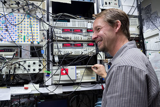
Andreas Heinrich
Andreas grew
up in Germany where he earned a PhD in the material properties of ternary compound
semiconductors, before joining IBM’s research Silicon Valley lab in Almaden as
a postdoctoral researcher in 1998. Today, he is the project leader for scanning
probe microscopy. He and his team work with single atoms, crucial to IBM's
research in the field of atomic-scale memory. In 2012, he was part of the team
that announced the creation of the
world's smallest magnetic memory bit, made of just 12 atoms.
This breakthrough
could lead to devices that have access to unprecedented levels of data storage.
To demonstrate their work with atoms, the scientists animated them using their
scanning tunneling microscope to make The World’s Smallest
Stop-Motion Film.
Anna Topol
Anna was also born in Europe, growing up in Poland before
completing her higher education in the U.S., including a PhD in Physics. Today,
she is a Distinguished Engineer and IBM Research’s Industry & Solutions CTO
group focused on technical
enablement and strategy for cloud and analytics solutions. She was also a part
of the team that led the research and development of three-dimensional
integrated circuits (3D IC).
The goal was to create a process for futureintegrated
circuit manufacturing by stacking silicon wafers or dies, and interconnecting
them vertically using through-silicon vias. Such connected components can behave
as a single device to achieve performance improvements at reduced power and with
a smaller footprint than conventional two dimensional processes.
What is your area of research?
Andreas Heinrich: The general area of my research is
called nanoscience or nanotechnology. In particular, we have the tools to
measure surfaces of materials (such as silicon or metals) with atomic-scale
spatial resolution. The tool we use is called a Scanning Tunneling Microscope
(STM). We like to put atoms on top of surfaces which we can then position with
atomic-scale precision. This [tool] allows us to build structures one atom at a
time, and build structures that do not exist in nature.
For the last few years we have been interested in the
properties of artificial magnetic structures in order to answer some
interesting questions: first, how small can we make a magnetic storage element
and what happens when it gets too small? We found that we could go as small as
12 atoms and demonstrate a magnetic Byte at the super-small scale. When
structures get even smaller, quantum mechanics takes over and it becomes
impossible to store magnetic information. Secondly, we are currently interested
in exploring such quantum systems on surfaces for quantum computation - a novel
way to potentially perform very fast computations.
Anna Topol: Throughout my career I focused on two
key areas. The first is related to information technology systems, from
integrated circuit devices, back-end metallization, and packaging, to server,
storage and network systems. And the second is related to Industry-specific
solutions, such as analytics-focused integrated hardware and software
capabilities designed to address specific industry challenges.
In addition to the 3D Integrated Circuit program, I had a privilege to
work with an IBM Research team that, in2004,
announced the
smallest functional 6T-SRAM cell
ever reported. The 2005 VLSI
paper on the design of this SRAM cell was recognized in 2015 as the most-cited among all papers presented
in Symposium on VLSI Technology from 2001-2014. This work was also a precursor
to the follow-on manufacturing enhancements of SRAM designs in computer processor chips. It led
to the higher system performance required for demanding applications like
banking and digital media.
My work then transitioned to more complex Information,
Computing and Communication systems. This led to my contributions to smarter computing
industry-specific work on why
infrastructure matters, where I first focused on Energy & Utilities, and
later on retail. My current interest is in cognitive computing, and its ability
to provide actionable insights.
When did you join IBM, and why?
AH: I performed research during my PhD in the field of STM. At
the time, the -IBM Research]-Almaden STM lab was led by Don Eigler, the
first person in history to move and control an individual atom. It was clear that that was the perfect
place to go.I met with Don a few times
before I convinced him to take me on board. It turned out to be a perfect job
for me, a great mix of engineering and science – and it has turned out to be
very successful research path.
AT: My PhD thesis was related to electroluminescent materials for
flat panel displays and head-mounted applications. Unfortunately by the end of
my PhD work it was clear that the market for flat panel displays would be
replaced by Liquid Crystal Displays (LCD), and not the thin film
electroluminescent displays I worked on.
I wanted to be hired by IBM Research, but at the time there
were no positions related directly to my PhD thesis or my M.S. work focused of
III-V materials. But I was patient, and even though I had offers from other
companies I stayed on as a post-doc at what
is now theColleges of Nanoscale Science
and Engineering at the SUNY Polytechnic Institute campus in Albany,
New York, waiting for the right opportunity at IBM
Research. To my delight I did not have to wait long. And after a few months, I
was hired in 2001 to work in the Microelectronics Advanced Materials and
Process Technology Group. My knowledge in the area of optoelectronics, previous
work in applied R&D, and strong microelectronics background in both device
and material science were a great match for my new position as an IBM Research
Staff Member.
How does your research matter in the
world?
AH: We are trying to figure out how small we can make devices for
data storage and computation. Rather than following Moore's Law, we are jumping
to the smallest length scale to begin with — the atomic scale. We are never
going to build things smaller than atoms. So we start with atoms and figure out
how the world works on that scale (there are a lot of open and interesting
questions in that realm) and how to potentially use our findings in future
devices.
AT: My original research focused on advanced interconnect
technology, and later on 3D IC. One of the key goals of this research was to
enable computing capabilities with higher performance with a smaller footprint.
The research in 3D IC was ground-breaking, as it literally opened a new
dimension to scientist and engineers – who now, instead of building in 2D (putting
the device circuit in one plane), started to construct devices and
heterogeneous circuits in 3D.
Anna with 3D Integrated Circuits
Today, the miniaturization trend is continuing, but in
addition to scaling the device and its underlying system architecture,
continuous innovation is being applied to other areas, including software defined
systems, enhanced network operations, and cloud services. A great real-world
example of this trend is how our cell phones have become smaller and lighter,
but offer higher processing power to run more apps and programs more effectively,
often via cloud services. Three-dimensional integrated systems challenged the
previously established design and way of processing microelectronic devices, highlighting
that often innovation comes not just from evolutionary steps but also from revolutionary
thinking.
What is your big-picture goal in this
research?
AH: I want to figure out whether we can use atoms on surfaces for
quantum computation. Quantum computation could revolutionize the world of
computation and our approach has some real advantages over other approaches. If
it is possible, it might be very impactful. And if it is not possible, we will
learn a lot of good basic science about why!
AT: The fundamental work on 3D IC technologies done by IBM and
others broke the status quo of building devices and integrated semiconductor
circuits in a two dimensional fashion. It resulted in a wave of new basic and
applied science accomplishments, from the creation of new semiconductor device design
structures and processes to build them, to rapid deployment of flexible
electronics.
With the pervasiveness of mobile technology, we have also entered
the era of wearable devices, computing at the edge, and the API economy. These new
information, computing and communication systems are far more advanced.
However, just like with 3D IC, we have to continue to look for ways to disrupt
the current methods of defining, designing and building these systems; to come
up with new solutions and enable new capabilities, and continue this remarkable
progress.
What does it mean to be named an AAAS
Fellow?
AH: Being a Fellow of a great scientific society is an honor. I
speak at a lot of conferences and adding this award to my bio helps convey to
audiences my dedication and contributions to the world of science.
AT: I am truly honored to have been recognized by the AAAS as a
Fellow since it is the world's largest general scientific society and publisher
of the globally renowned scientific journal Science.This is an acknowledgement of the impact of
3D IC technology and affirmation for many who have contributed to research and
development in this area.
What's the best advice you've received
in your career?
AH: Don't accept ‘No’ as an answer. On the other hand, as a group
leader: try to protect your time and say ‘No’ as often as you can to be able to
focus onimportant tasks.
AT: Perseverance and willingness to take risks is incredibly
important to the success of research and our ability to innovate.