 |
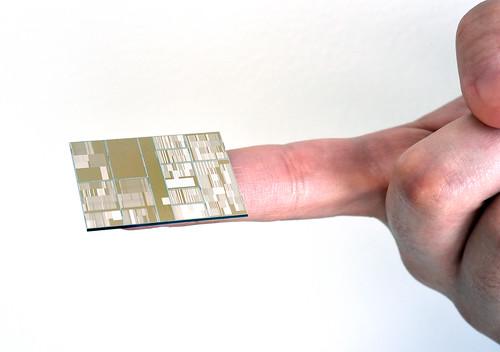
| IBM 7nm node test chip |
Industry experts consider 7 nanometer (nm) technology crucial to
meeting the anticipated demands of future cloud computing and big data systems,
cognitive computing, mobile products and other emerging technologies.
Microprocessors utilizing 22 nm and 14 nm technology power today’s
servers, cloud data centers and mobile devices, and 10 nm technology is well on
the way to becoming a mature technology, but the challenges dramatically
increase when going below 7 nm or even 5 nm.
At dimensions below 5 nm it becomes increasingly difficult to
achieve reasonably high on/off current ratios, mainly because of increasing
leakage paths and less control over the doping atoms. To explain the challenge,
consider a leaky water faucet – even after closing the valve as far as possible,
water continues to drip. This is similar to today’s transistor, in that energy
is constantly "leaking" or being lost or wasted in the off-state. For
these reasons, scientists around the world are exploring novel materials
including carbon nanotubes, graphene, 2D layered materials, phase-change
materials or single molecules to discover novel type of switching mechanisms
with enhanced control over transport at nanometer dimensions.
Appearing today in the peer-review journal NatureNanotechnology, scientists at IBM Research, the University of Zurich and
the University of Vienna are reporting on a novel concept to modulate the current
through a less-than-3 nm long molecule by more than three orders of magnitude –
a critical step to control transport for future electric circuits, with
applications in signal processing, logic data manipulation, data storage or
neuromorphic networks.
Let’s get straight to the most pressing
question, have you discovered the so-called “next switch”?
 |
| Emanuel Loertscher |
Emanuel Lörtscher (EL): I wouldn’t say so because of the
following reason: In our work, we employ redox-active metal centers embodied in
a single molecular compound. The novelty is that the charge-state of these 3 nm
long molecules can be addressed solely by the external field present in a
simple two terminal geometry, changing the conductance by more than three
orders of magnitude simply by adding one extra charge onto the molecule. This abrupt
switching behavior and its large influence on transport are quite astonishing for
a molecular-intrinsic mechanism that does furthermore not require a gate
electrode, like in case of a standard CMOS transistor. In that sense, such
functional molecular compounds are very promising switches.
For the ideal “next switch” however, substantially higher “on”
currents are needed, a requirement that a single molecule cannot fulfill and
will never as its intrinsic degrees of freedom – the intrinsic functionality –
get lost upon coupling it too strongly to electrodes. Ensembles of molecules however,
could potentially do that task and may serve as the active “next switching
component,” causing switching and hysteresis for memory applications. Even a few
hundred molecules will occupy a footprint which is still sufficiently small to
be technologically attractive. The well-defined, microscopic integration of
multiple molecules into circuits is however, still a vision.
In the paper you state that have
achieved an abrupt switching ratio with high-to-low current of more than 1,000,
which outperformes all previously explored molecular-intrinsic
conductance-switching mechanisms. What was the previous level and why is this
ratio so important?
EL: For electronic devices, the high-to-low current ratio defines
in principle the possible range of applications –
the higher the “better” for circuit functionality, fault tolerance, storage contrast, etc. Usually in
single molecules, the conductance could be varied only by a factor of 3 – 50, employing
the existing mechanisms such as rotation or conformational changes.
To go
beyond that level and to reach technologically relevant high-to-low ratios of
1,000, more advanced mechanisms had to be developed. We employ intrinsic charge
states of redox-active metal centers that we place directly into the transport
pathway of electrons to achieve the largest possible influence on the
conductance – a concept that has been optimized over the years and finally
realized by our chemistry partners form the University of Zurich. On the
sub-5 nm range, the performance achieved in these organometallic
compounds can compete even with other technologies that usually suffer from
severe scaling limitations.
 |
Abrupt switching ratio with high-to-low current of more than 1,000
was achieved |
It appears that the “secret sauce"
to your design was the introduction of molybdenum. How did you decide to
include it in your device?
EL: This is correct. The big performance improvements
arose by using molybdenum as central metal atom. This was pure instinct of
the chemists combined with physicist’s hope to cause more pronounced effects
due to the high magnetic anisotropy of Mo (molybdenum). The abrupt behavior found, however,
made it hard to understand exactly why molybdenum causes such unique effects
– distinctly different from Fe (iron) and Ru (ruthenium).
Calculations performed by our colleagues
from the University of Vienna finally provided a microscopic picture that
agreed excellently with our experimental findings: The Mo has a spin-polarized
ground state, which creates a localized molecular orbital that is weakly
coupled and can be charged by a slow, decoherent hopping process, resulting in
the huge switching and hysteresis we discovered experimentally. So in simple terms,
we use quantum mechanical effects to create a highly functional molecule acting
as an efficient current switch and storage element with unprecedented
performance.
In the summary you cite future memory
applications for your device. What are the advantages of using molecules for
that task?
EL: This work represents fundamental research that
assesses the potential of novel concepts for future electronics. Talking about
applications is therefore quite speculative, keeping all the technical and
economical boundary conditions in mind. The large conductance alternation and
the hysteresis caused by adding a single extra charge to the molecule, however,
is a finding with large potential for various applications, namely in data
storage or neuromorphic networks, simply by its basic two-terminal addressing
and non-linear electrical response function.
In fact, charge and spin states in molecules are quantum
mechanical mechanisms that can ideally be employed to provide novel complex functionality not used in today’s transistor technology. These capabilities can be tailored and embodied in scaled compounds
that can all be produced identically, due to the chemical synthesis used as a cheap,
bottom-up fabrication process with sub-atomic control.
What’s next for your research?
EL:
As we discussed above, molecular compounds have truly large potential to be
used as highly functional electronic building blocks. But their reliable
implementation represents the main show stopper for practical usage since the
dawn of molecular electronic concepts 40 years ago. In order to overcome this
technological hurdle, we are currently working (in the framework of NCCR MSE) on
implementing ensembles of molecules reliably in nanopores, on a solid-state and
wafer-scale platform for robust operation under ambient conditions.
This will
keep us busy for the next few years – but all this incremental success, together
with the new horizons IBM is currently looking at, keep us motivated every day.
Labels: IBM Research - Zurich, microprocessor, nanotechnology

