IBM scientists in Zurich
and Yorktown Heights, New York have unveiled a breakthrough approach in two publications for
growing and integrating nano-sized III-V semiconductor devices on silicon. Both
papers offer the microelectronics industry a possible answer to the long term
challenge of creating a new powerful and energy efficient, yet smaller
transistor to pave path for technology scaling for advanced CMOS nodes.
Researchers from the IBM’s Materials Integration and Nanoscale Devices group demonstrated a novel, robust
and yet versatile approach for integrating III-V compound semiconductor
crystals on silicon wafers – a novel and an important step toward making
chips smaller and more powerful at lower power density.
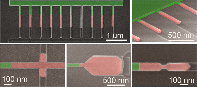 |
Scanning electron
microscope images of single crystal structures fabricated
using template-assisted selective epitaxy. For better visibility, the silicon
is colored in green, and the compound semiconductor in red. |
The technique developed can
be used to combine III-V materials, including indium, gallium and arsenide (InGaAs),
with silicon germanium technology to create CMOS chips. It is fully compatible
with current high volume chip fabrication technology, making it economically
viable for chip manufacturers.
The first paper was
published last week in the journal Applied Physics Letters by
lead author Heinz Schmid who describes the crystal growth starting from a small
area and evolving into a much larger, defect-free crystal. In this so-called
template-assisted selective epitaxy the oxide templates are defined and
selectively filled via epitaxy to create arbitrary shaped III-V semiconductors
such as nanowires, cross junctions, nanostructures containing constrictions and
3D stacked nanowires.
Using this
small seed area epitaxy, today at the VLSI Symposium in Kyoto, IBM scientist Lukas Czornomaz is presenting a solution for large scale and controlled integration
of high quality InGaAs on bulk Silcon (Si) which is based on standard CMOS process
modules. Gate-first CMOS-compatible InGaAs FinFETs on Si with excellent
performance have been demonstrated and integrated seamlessly in a CMOS
manufacturing flow.
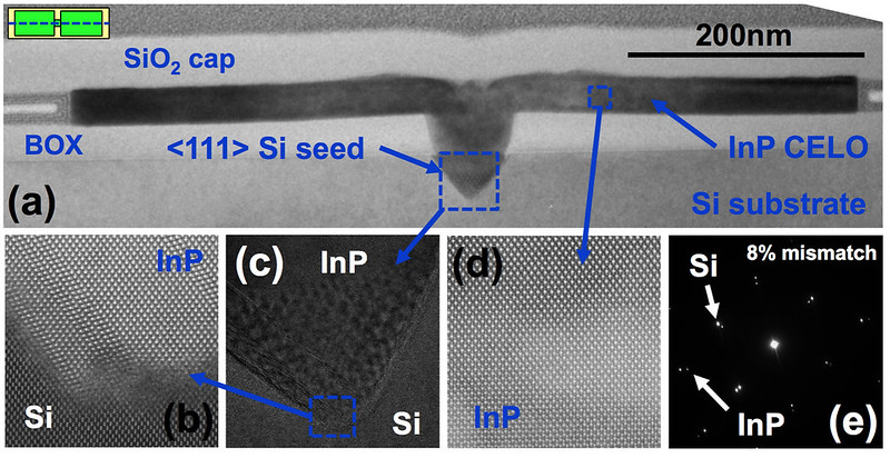 |
Cross-sectional TEM view along InP integrated on Si using the new technique.
High number of defects are observed at the seed region by
HR-STEM(b)/TEM(c) mostly consisting of stacking faults. Away from the seed,
a perfect lattice structure is observed with 8% mismatch to Si corresponding to fully relaxed InP (d,e). |
Integrating high quality III-V
materials on silicon is critical for getting the benefit of higher electron
mobility to build transistors with improved power and performance for technology
scaling at 7 nm and beyond. Unfortunately, growing III-V materials on 300 mm
silicon substrates isn’t easy and often produces wafers with so many
defects that they are rendered useless.
The described novel
epitaxy and integration process allows the materials to be grown precisely with
a low number of defects on the wafer position where they are needed and
therefore represent a significant, economical and manufacturable breakthrough
towards the introduction of high-mobility channels into advanced CMOS nodes.
The new technique may also
impact photonics on silicon, with active photonic components integrated
seamlessly with electronics for greater functionality.
Both papers are part of IBM’s $3 billion, five year investment to push the limits of silicon technology to 7 nanometers and below. More specifically, IBM scientists are motivated to integrate III-V materials on silicon for faster and more powerful devices. IBM is betting that future chips made of these materials will create more energy efficient and powerful cloud data centers and consumer devices.
Labels: finFET, III-V, nano, photonics, silicon, transistor